科研与工业产品
光通信产品
技术方案产品
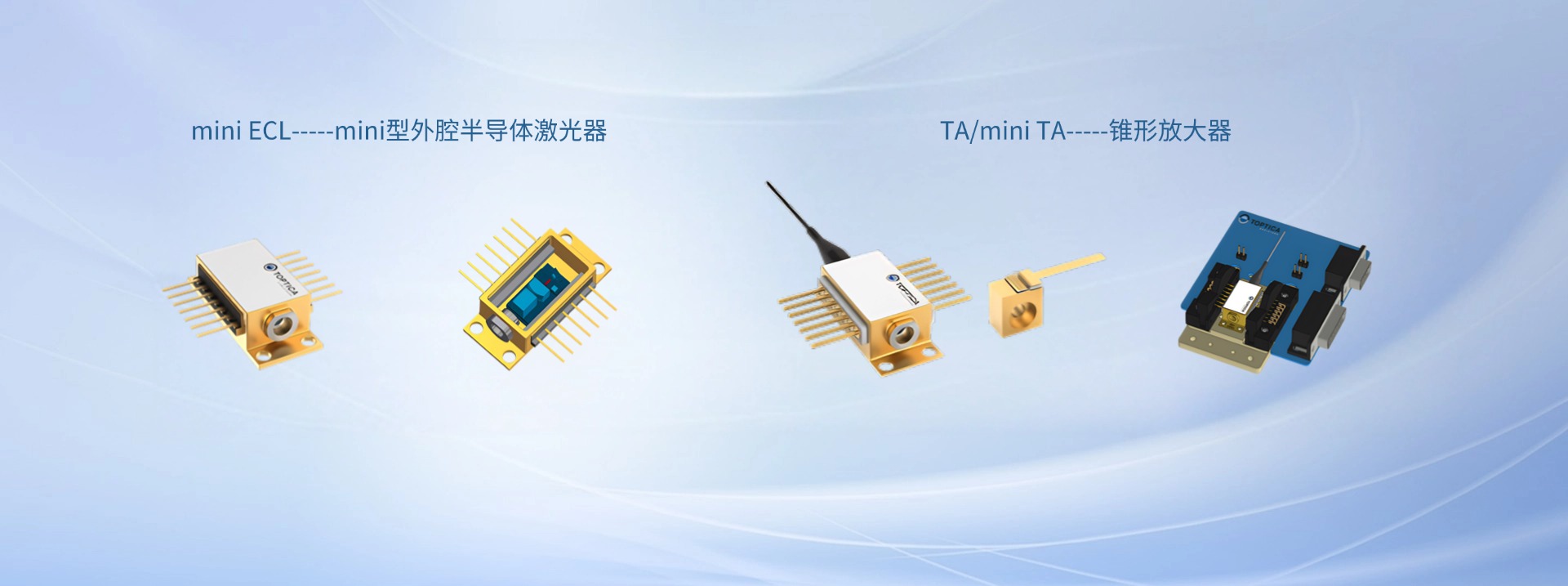
光源
探测器、相机
电子控制
光调制
测量模块及设备
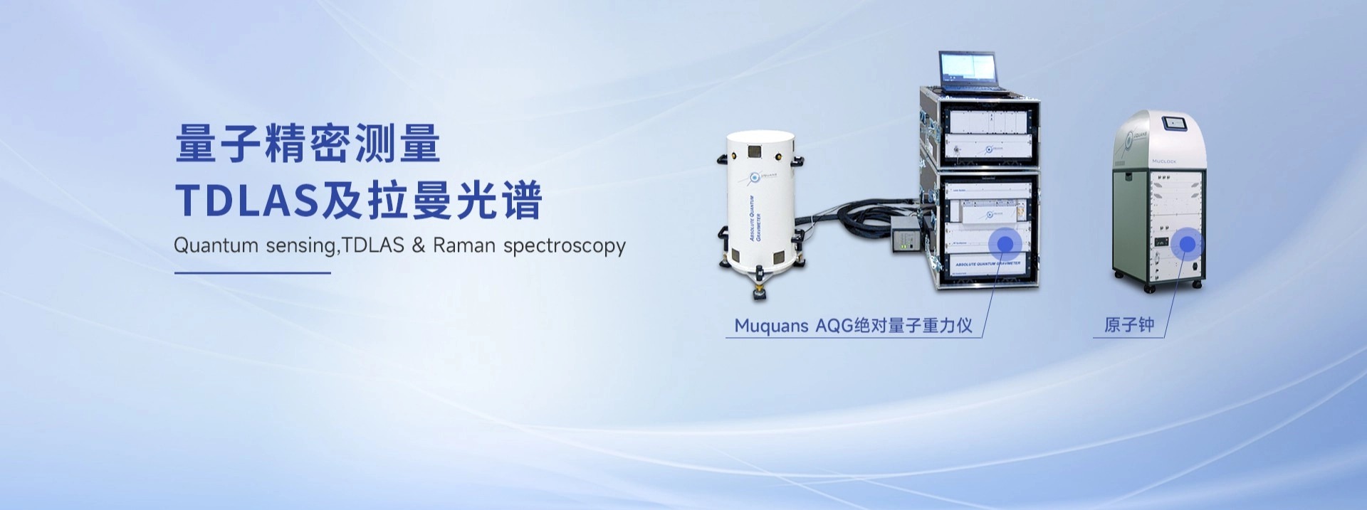
量子科技用器件/模块/设备
特种光纤
光学无源器件
光栅、晶体
气体池
配件
太赫兹器件及模组
微米纳米定位平台
半导体材料
光通信材料
光通信器件与模块
生产与测试设备
通信综合系统
测试与分析仪器
光通信有源模块制造
无源器件制造
光传输网络模块
光通信自动化设备
网络、安全及应用交付
最新方案
可调半导体吸收光谱方案
冷原子用激光系统方案
射频性能测试方案
组件封装解决方案
芯片工艺流程方案
激光稳频解决方案


 400-169-1558
  info@photonteck.com
 微信公众号
微信公众号